
In this fast-changing world of technology is the Internet of Things (IoT), a revolutionary example of an interconnectedness and an automation phenomenon. This article scrutinizes the trends in VLSI design for IoT which impact industries by presenting a new age of innovation and intelligent integration between software modules and front-end hardware. The advent of VLSI design engineering has ushered us into the intelligent devices era in which now can sense, process, and take action to data in real-time like in agriculture, health industry, transportation, and manufacturing sectors. One of the key factors in the proliferation of IoT technologies is the VLSI designer’s use of sophisticated semiconductor fabrication techniques and design approaches. Their contributions are facilitating the development of IoT solutions that provide a myriad of benefits, namely enhancements in efficiency, convenience, and safety.
Among the top-dog countries in regular hardware design in USA constitutes a global leader with proven chips and research institutions, which are key to the innovation of VLSI chip design.
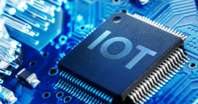
Evolution of VLSI design
The history of the VLSI process is a story of continuously amassing more doing into smaller chips. Through the years, following the semiconductor manufacturing processes progressed, and allowed to simultaneously bring millions to billions of transistors on the chip surface. The exponential increase in the performance and shrinkage of the size has promoted IoT devices with incredulous features whereby the connections are regarded as seamless, and the functionality seems intelligent. VLSI will be the force that will keep introducing innovation to the realm of IoT and not stop until the fullest complexity and performance of chips are achieved; thus, the digital world will allow experiencing all the comfort that can be provided.
See also: How to Calculate the Server Cost for Your Mobile Application
The Rise of IoT and its challenges
The Internet of Things has a main idea in its use of interconnected devices, thus allowing them to gather, analyze and act upon data without human involvement. Even though constructing IoT systems carries specific difficulties, these can be easily overcome with the use of modern tools and instruments.
VLSI has a surgical design that targets these above-mentioned challenges with optimization of the hardware architecture to specifically implement algorithms for action, successful communication between sensors, actuators, and processing units is ensured. Through ensuring the implementation of equal measures for performance, power consumption, and area profiles, very-large-scale integration (VLSI) engineers provide IoT designers with the tools to create systems which are both flexible and reliable while at the same time allowing for multi-application diversification.
Hardware designs
Companies have a unique opportunity to show effective approaches for bringing to the market not just sophisticated software with localized versions but also hardware products. Especially known for the solidity of its support infrastructure, this area becomes the breeding ground for new creative ideas through researchers in it thus, the semiconductor industry is brought to an unmatchable summit at the end.
The Role of VLSI in IoT
VLSI design is an important element that determines how much room for development can be achieved through the IoT. Through synthesizing multiple intricate functions into one chip, VLSI transforms the development of compact, least powerful and capable devices that undertake numerous tasks, such as simultaneously sensing data, performing analytics in real-time and communicating.
Key aspects of VLSI design for IoT
Integration of sensors and actuators
VLSI design opens up the possibility of including sensing and actuation elements as subsets of a chip so that these devices can communicate well with the real world. This cuts down on total volume as well requiring less energy to be consumed inside the IoT devices hence, such gadgets are made to operate in different places without any complications.
IC packaging design services
The reason for this in the field of VLSI design, IC packaging is one the most critical factors that guarantee semiconductor devices are reliable and performant. IC packaging design services bring into play a wide range of tasks which cover the issues connected with package selection, thermal management, signal integrity analysis, and reliability testing. These services are built-in features that foster the effective design of IoT devices in consideration of form factor, power dissipation, and practical electrical performance, especially for those with stringent sizing and power restrictions.
Low-Power Design Techniques
Efficiency of power is highly fortunate in IoT tools, especially when such tools are powered by batteries or harvesting energy. VLSI System-level designers work with the first order of low-level power techniques such as Dynamic Voltage and Frequency Scaling, clock gating, and power gating, producing more power-efficient devices with no performance sacrifice.
Real-Time processing capabilities
Since many IoT applications are data-driven, data processing takes place in real-time helping with quick decision-making and responsiveness, else it may be impossible to make any decision or respond at the right time.
VLSI design has on board all features for the customized processing units that are used in IoT. The specialized processing units can range from Digital signal processors to neural network accelerators.
Wireless communication interfaces
IoT devices use Wi-Fi or other wireless communication protocols for data transmission from their devices to centre systems. The high- and low-rate communication protocols have their respective advantages in the range, data rate, power consumption, and networking scalability, and this allows designers to construct characteristic solutions tailored to unique use cases and requirements. Through these wireless arrangements, digital designers make it possible for IoT devices to stay in mutual communication, via bending back systems, which implies real-time data transfers including advanced functionalities such as remote monitoring, remote control and analytics.
Security and trustworthiness
Within the cyber security field, ever alertness is critical since connected devices can pose a threat or have consequences. Security is the fundamental concern to view upon because of the overwhelming spread of networked devices, and possible negative consequences. VLSI designers take the hardware level and include cryptography processors, secure startup flags, and uninhabitable features which are dedicated to securing data and confirming the consistency of the IoT systems. With continually improving technology, enabling quality and strength of security protocols becomes more and more of top priority.
Conclusion
Therefore, VLSI design is not limited to working more integrated circuits on the chip; rather it fullest design of chips, blending hardware and software features for intelligent solutions which ultimately enable organizations and people to take full potential of the Internet of Things. Semiconductor engineering services occupy a core position in the drive to achieve these ambitions. Providers of these services offer a set of competencies and infrastructure that are required to develop high-end semiconductor devices. As the IoT network is ever more decorated and affected, chip design will take centre stage and hence, how smart and connected devices will function in physically in our daily lives.